
关注 “环球资源外贸” 官方微信,获取实时外贸资讯
Product Information
Key Specifications/ Special Features
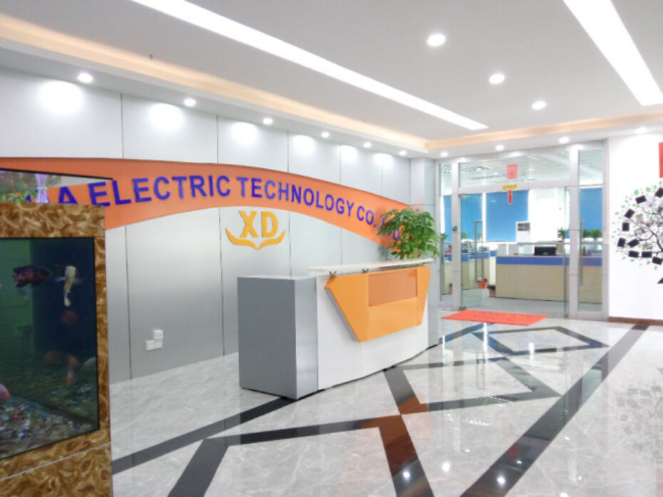
Welcome to XingDa Electric Technology Co.,Ltd
Xindaxing Electric Technology Co.,LTd
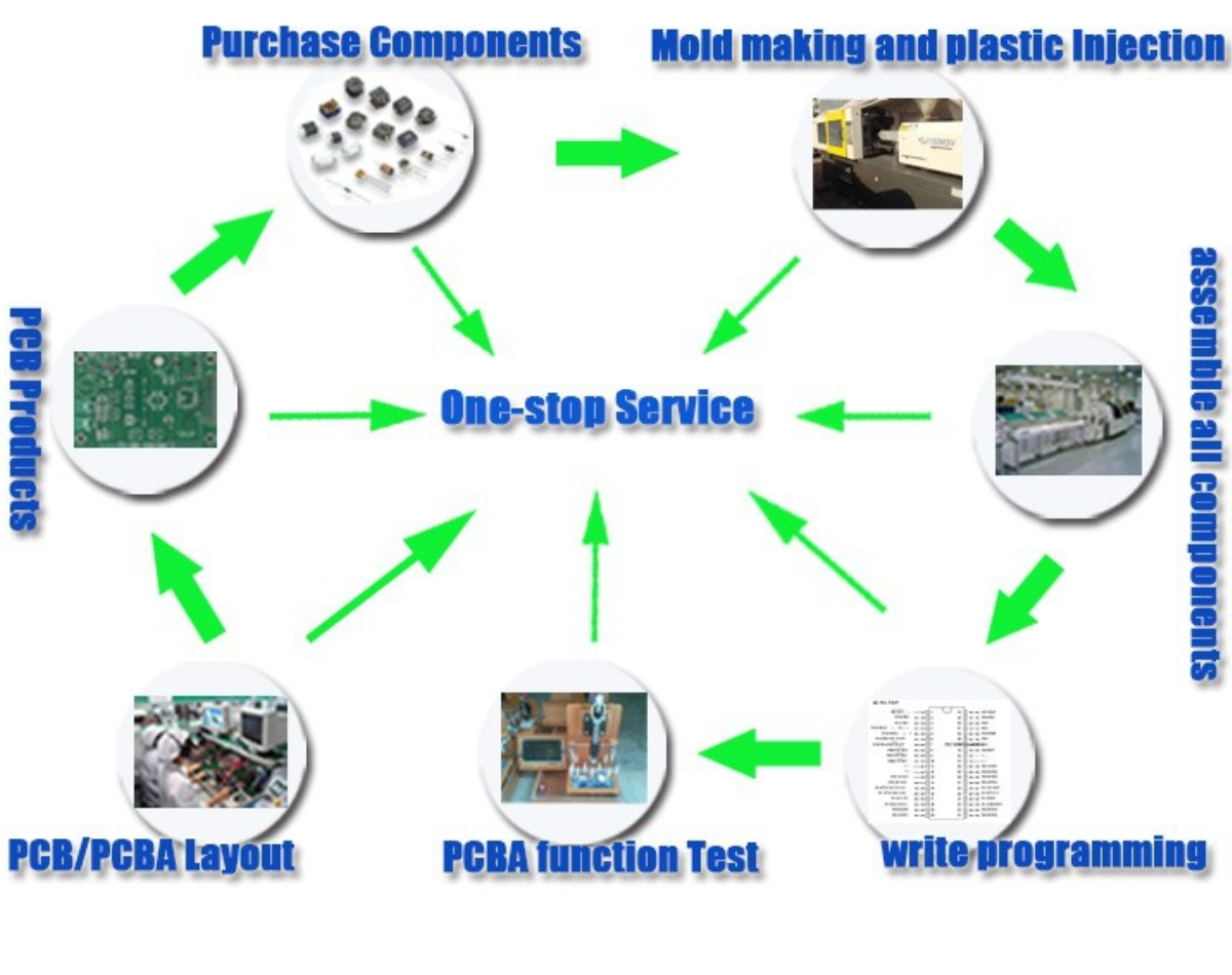
Our Services
We can provide one-stop service:
1. PCB circuit boards.
2. E-test.
3.Electronic components purchasing.
4. PCB assembly: available on SMT, BGA, DIP.
5. PCBA function test.
6. Enclosure assembly.
PCB product Capacity
| PCB Manufacture Capacity | |
| Item | Specification |
| Material | FR-4, FR1,FR2; CEM-1, CEM-3,Rogers, Teflon,Arlon,Aluminum Base, Copper Base,Ceramic, Crockery, etc. |
| Remarks | High Tg CCL is Available(Tg>=170℃) |
| Finish Board Thickness | 0.2 mm-6.00mm(8mil-126mil) |
| Surface Finish | Gold finger(>=0.13um), Immersion Gold(0.025-0075um), Plating Gold(0.025-3.0um), HASL(5-20um), OSP(0.2-0.5um) |
| Shape | Routing,Punch,V-cut,Chamfer |
| Surface Treatment | Solder Mask(black, green, white, red, blue, thickness>=12um, Block, BGA) |
| Silkscreen(black, yellow, white) | |
| Peel able-mask(red, blue, thickness>=300um) | |
| Minimum Core | 0.075mm(3mil) |
| Copper Thickness | 1/2 oz min; 12oz max |
| Min Trace Width & Line Spacing | 0.075mm/0.075mm(3mil/3mil) |
| Min Hole Diameter for CNC Drilling | 0.1mm(4mil) |
| Min Hole Diameter for Punching | 0.6mm(35mil) |
| Biggest panel size | 610mm * 508mm |
| Hole Position | +/-0.075mm(3mil) CNC Drilling |
| Conductor Width(W) | +/-0.05mm(2mil) or +/-20% of original |
| Hole Diameter(H) | PTHL:+/-0.075mm(3mil) |
| Non PTHL:+/-0.05mm(2mil) | |
| Outline Tolerance | +/-0.1mm(4mil) CNC Routing |
| Warp & Twist | 0.70% |
| Insulation Resistance | 10Kohm-20Mohm |
| Conductivity | <50ohm |
| Test Voltage | 10-300V |
| Panel Size | 110 x 100mm(min) |
| 660 x 600mm(max) | |
| Layer-layer misregistration | 4 layers:0.15mm(6mil)max |
| 6 layers:0.25mm(10mil)max | |
| Min spacing between hole edge to circuitry pattern of an inner layer | 0.25mm(10mil) |
| Min spacing between board outline to circuitry pattern of an inner layer | 0.25mm(10mil) |
| Board thickness tolerance | 4 layers:+/-0.13mm(5mil) |
Flexible PCB product Capacity
| FPC Tech Specification | |
| Items | Capabilities |
| Layers | FPC:1 to 6 Layers, Rigid Flex: 2 to 10 Layers |
| Regular Base Materials | Kapton,Polyimide(PI), Polyester(PET), FR4 |
| Base Copper Thickness | 1/3 oz to 8oz |
| Regular Base Material Thickness | 12.5um to 50um(FPC) |
| 0.1mm to 3.2mm(Rigid) | |
| Regular Coverlay Thickness | 27um to 50um |
| Regular Adhesive Thickness | 12um to 25um |
| Blind or Buried Vias | Yes |
| Impedance Control | Yes |
| Min.Line Width/Spacing | 0.04mm/0.04mm |
| Surface Finishing | Electroplate Ni/Au(Flash gold/Soft gold/Hard gold), ENIG, HASL, Immersion Tin,OSP |
| Outline Fabrication | Die cut, laser cut, CNC routing, V-scoring |
| Hole to edge(Hard tool/Die Cut) | ±0.1/±0.2mm |
| Edge to edge(Hard tool/Die Cut) | ±0.05/±0.2mm |
| Circuit to edge(Hard tool/Die Cut) | ±0.07/±0.2mm |
PCB Assembly(SMT) Product Capacity
| SMT Capacity | |
| SMT Item | Capacity |
| PCB Max. size | 510mm*1200mm(SMT) |
| Chip component | 0201, 0402, 0603, 0805, 1206 package |
| Min.pin space of IC | 0.1mm |
| Min. space of BGA | 0.1mm |
| Max.precision of IC assembly | ±0.01mm |
| Assembly capacity | ≥8 million piots/day |
| DIP capacity | 6 DIP production lines |
| Assembly testing | Bridge test,AOI test, X-Ray test, ICT(In Circuit Test),FCT(Functional Circuit Test) |
FCT(Functional Circuit Test) | Current test, voltage test, high temperature and low temperature test,Drop Impact Test,aging test,water proof test,leakage-proof test and etc.Different test can be done according to your requirement. |
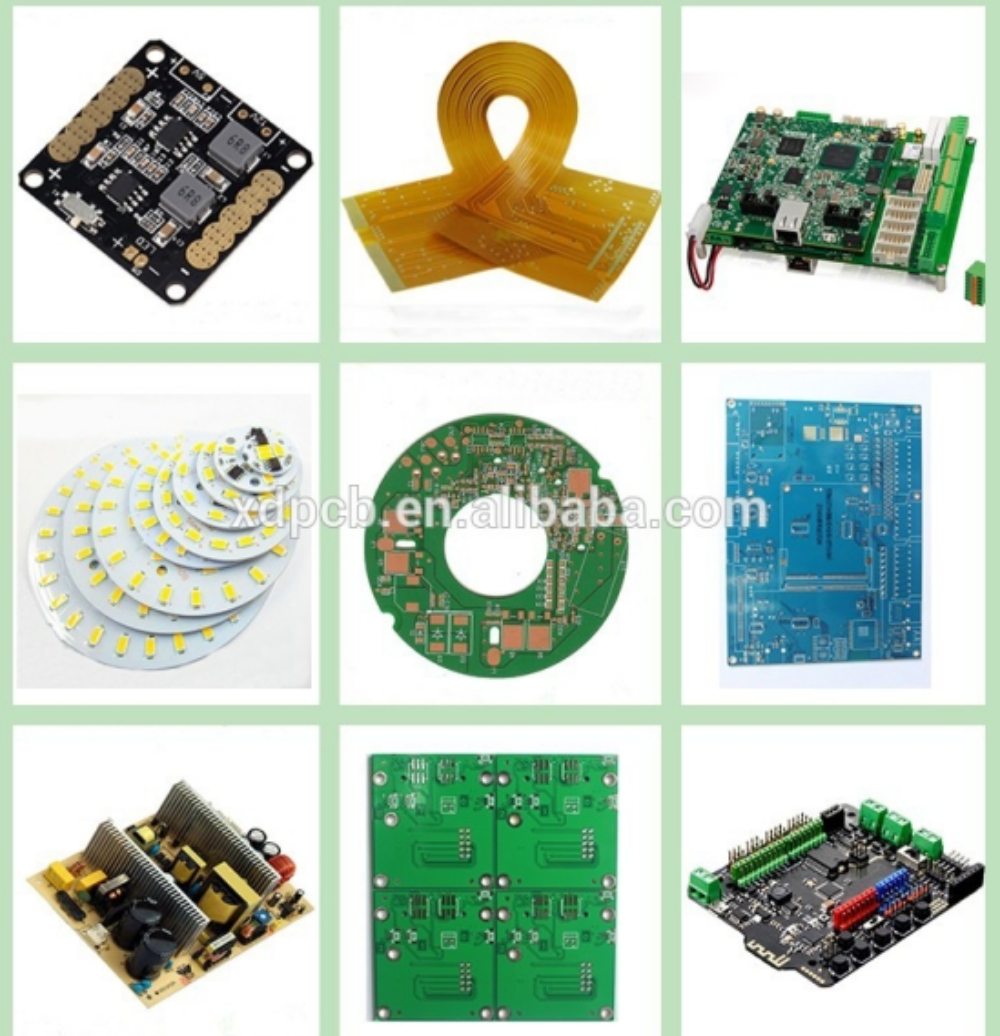
Related Products
High Quality PCB, FPC and PCBA!
View of Factory

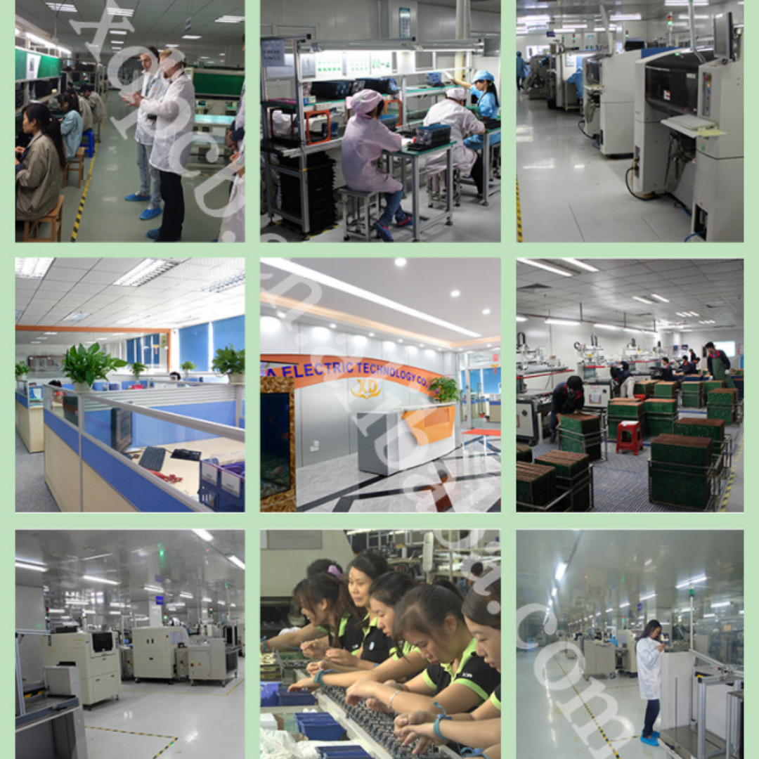
Customer visiting

Exhibition Show:

FAQ
Q1:Are you a factory or trade company?
A: XingDa is a PCB/FPC/PCBA manufacturer/factory. We pecialize in PCB/PCBs Board for 10 years.
Q2:Is my PCB file safe if I send it to you for manufacturing?
A: We respect customer's design authority and will never manufacture PCB for someone else without your permission. NDA is acceptable.
Q3:What payment do you accept ?
A: TT/ Western Union/ Paypal/ Unistream.
Q4: What's your shipping way ?
A: 1. We have our own forwarder to ship goods by DHL, UPS, FEDEX, TNT,EMS.
2. If you have your own forwarder, we can cooperate with them.
Q5: How about the MOQ?
A: For PCB: 1 pcs
For PCBA: 1pcs
Packaging & Shipping


Welcome to XingDa Electric Technology Co.,Ltd
Xindaxing Electric Technology Co.,LTd
Our Services
We can provide one-stop service:
1. PCB circuit boards.
2. E-test.
3.Electronic components purchasing.
4. PCB assembly: available on SMT, BGA, DIP.
5. PCBA function test.
6. Enclosure assembly.
PCB product Capacity
| PCB Manufacture Capacity | |
| Item | Specification |
| Material | FR-4, FR1,FR2; CEM-1, CEM-3,Rogers, Teflon,Arlon,Aluminum Base, Copper Base,Ceramic, Crockery, etc. |
| Remarks | High Tg CCL is Available(Tg>=170℃) |
| Finish Board Thickness | 0.2 mm-6.00mm(8mil-126mil) |
| Surface Finish | Gold finger(>=0.13um), Immersion Gold(0.025-0075um), Plating Gold(0.025-3.0um), HASL(5-20um), OSP(0.2-0.5um) |
| Shape | Routing,Punch,V-cut,Chamfer |
| Surface Treatment | Solder Mask(black, green, white, red, blue, thickness>=12um, Block, BGA) |
| Silkscreen(black, yellow, white) | |
| Peel able-mask(red, blue, thickness>=300um) | |
| Minimum Core | 0.075mm(3mil) |
| Copper Thickness | 1/2 oz min; 12oz max |
| Min Trace Width & Line Spacing | 0.075mm/0.075mm(3mil/3mil) |
| Min Hole Diameter for CNC Drilling | 0.1mm(4mil) |
| Min Hole Diameter for Punching | 0.6mm(35mil) |
| Biggest panel size | 610mm * 508mm |
| Hole Position | +/-0.075mm(3mil) CNC Drilling |
| Conductor Width(W) | +/-0.05mm(2mil) or +/-20% of original |
| Hole Diameter(H) | PTHL:+/-0.075mm(3mil) |
| Non PTHL:+/-0.05mm(2mil) | |
| Outline Tolerance | +/-0.1mm(4mil) CNC Routing |
| Warp & Twist | 0.70% |
| Insulation Resistance | 10Kohm-20Mohm |
| Conductivity | <50ohm |
| Test Voltage | 10-300V |
| Panel Size | 110 x 100mm(min) |
| 660 x 600mm(max) | |
| Layer-layer misregistration | 4 layers:0.15mm(6mil)max |
| 6 layers:0.25mm(10mil)max | |
| Min spacing between hole edge to circuitry pattern of an inner layer | 0.25mm(10mil) |
| Min spacing between board outline to circuitry pattern of an inner layer | 0.25mm(10mil) |
| Board thickness tolerance | 4 layers:+/-0.13mm(5mil) |
Flexible PCB product Capacity
| FPC Tech Specification | |
| Items | Capabilities |
| Layers | FPC:1 to 6 Layers, Rigid Flex: 2 to 10 Layers |
| Regular Base Materials | Kapton,Polyimide(PI), Polyester(PET), FR4 |
| Base Copper Thickness | 1/3 oz to 8oz |
| Regular Base Material Thickness | 12.5um to 50um(FPC) |
| 0.1mm to 3.2mm(Rigid) | |
| Regular Coverlay Thickness | 27um to 50um |
| Regular Adhesive Thickness | 12um to 25um |
| Blind or Buried Vias | Yes |
| Impedance Control | Yes |
| Min.Line Width/Spacing | 0.04mm/0.04mm |
| Surface Finishing | Electroplate Ni/Au(Flash gold/Soft gold/Hard gold), ENIG, HASL, Immersion Tin,OSP |
| Outline Fabrication | Die cut, laser cut, CNC routing, V-scoring |
| Hole to edge(Hard tool/Die Cut) | ±0.1/±0.2mm |
| Edge to edge(Hard tool/Die Cut) | ±0.05/±0.2mm |
| Circuit to edge(Hard tool/Die Cut) | ±0.07/±0.2mm |
PCB Assembly(SMT) Product Capacity
| SMT Capacity | |
| SMT Item | Capacity |
| PCB Max. size | 510mm*1200mm(SMT) |
| Chip component | 0201, 0402, 0603, 0805, 1206 package |
| Min.pin space of IC | 0.1mm |
| Min. space of BGA | 0.1mm |
| Max.precision of IC assembly | ±0.01mm |
| Assembly capacity | ≥8 million piots/day |
| DIP capacity | 6 DIP production lines |
| Assembly testing | Bridge test,AOI test, X-Ray test, ICT(In Circuit Test),FCT(Functional Circuit Test) |
FCT(Functional Circuit Test) | Current test, voltage test, high temperature and low temperature test,Drop Impact Test,aging test,water proof test,leakage-proof test and etc.Different test can be done according to your requirement. |
Related Products
High Quality PCB, FPC and PCBA!
View of Factory
Customer visiting
Exhibition Show:
FAQ
Q1:Are you a factory or trade company?
A: XingDa is a PCB/FPC/PCBA manufacturer/factory. We pecialize in PCB/PCBs Board for 10 years.
Q2:Is my PCB file safe if I send it to you for manufacturing?
A: We respect customer's design authority and will never manufacture PCB for someone else without your permission. NDA is acceptable.
Q3:What payment do you accept ?
A: TT/ Western Union/ Paypal/ Unistream.
Q4: What's your shipping way ?
A: 1. We have our own forwarder to ship goods by DHL, UPS, FEDEX, TNT,EMS.
2. If you have your own forwarder, we can cooperate with them.
Q5: How about the MOQ?
A: For PCB: 1 pcs
For PCBA: 1pcs
Packaging & Shipping
 ,Manufacturer ,Other