
关注 “环球资源外贸” 官方微信,获取实时外贸资讯
Product Information
Key Specifications/ Special Features
Industrial HMI device PCBA OEM electronic printed circuit board pcb assembly pcb board customized pcba
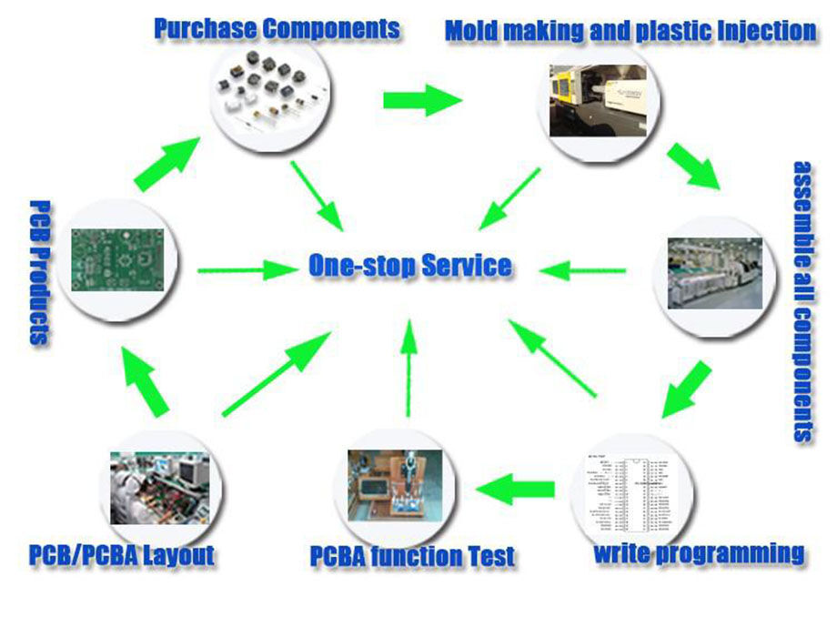
Xing Da Electric Technology Co.,Ltd can provide one-stop service:
1. PCB layout
2. PCB manufacturing(1-38layers)
3. All electronic components purchasing
4. PCB assembling
5. PCBA function testing
6. Make mold of housing
7. Make housing and housing assembly.

PCB Product Capacity
| Item | Specification |
| Material | FR-4,FR1, CEM-1, CEM-3,Aluminum, Ceramic, Metal-backed Laminate, etc.Also make Crockery, Taconic, Rogers PCBs etc. |
| Remarks | High Tg CCL is Available(Tg>=180℃) |
| Finish Board Thickness | 0.2 mm-6.00mm(8mil-126mil) |
| Surface Finish | Gold finger(>=0.13um), Immersion Gold(0.025-0075um), Plating Gold(0.025-3.0um), HASL(5-20um), OSP(0.2-0.5um) |
| Shape | Routing、Punch、V-cut、Chamfer |
| Surface Treatment | Solder Mask(black, green, white, red, blue, thickness>=12um, Block, BGA) |
| Silkscreen(black, yellow, white) | |
| Peel able-mask(red, blue, thickness>=300um) | |
| Minimum Core | 0.075mm(3mil) |
| Copper Thickness | 1/2 oz min; 12oz max |
| Min Trace Width & Line Spacing | 0.075mm/0.0.075mm(3mil/3mil) |
| Min Hole Diameter for CNC Drilling | 0.1mm(4mil) |
| Min Hole Diameter for Punching | 0.6mm(35mil) |
| Biggest panel size | 610mm * 508mm |
| Hole Position | +/-0.075mm(3mil) CNC Drilling |
| Conductor Width(W) | +/-0.05mm(2mil) or +/-20% of original |
| Hole Diameter(H) | PTHL:+/-0.075mm(3mil) |
| Non PTHL:+/-0.05mm(2mil) | |
| Outline Tolerance | +/-0.1mm(5mil) CNC Routing |
| Warp & Twist | 0.70% |
| Insulation Resistance | 10Kohm-20Mohm |
| Conductivity | <50ohm |
| Test Voltage | 10-300V |
| Panel Size | 110 x 100mm(min) |
| 660 x 600mm(max) | |
| Layer-layer misregistration | 4 layers:0.15mm(6mil)max |
| 6 layers:0.25mm(10mil)max | |
| Min spacing between hole edge to circuitry pattern of an inner layer | 0.25mm(10mil) |
| Min spacing between board outline to circuitry pattern of an inner layer | 0.25mm(10mil) |
| Board thickness tolerance | 4 layers:+/-0.13mm(5mil) |
Flexible PCB Capacity
| FPC Tech Specification | |
| Items | Capabilities |
| Layers | FPC:1 to 6 Layers, Rigid Flex: 2 to 10 Layers |
| Regular Base Materials | Kapton,Polyimide(PI), Polyester(PET) |
| Base Copper Thickness | 1/3 oz to 8oz |
| Regular Base Material Thickness | 12.5um to 50um(FPC) |
| 0.1mm to 3.2mm(Rigid) | |
| Regular Coverlay Thickness | 27um to 50um |
| Regular Adhesive Thickness | 12um to 25um |
| Blind or Buried Vias | Yes |
| Impedance Control | Yes |
| Min.Line Width/Spacing | 0.04mm/0.04mm |
| Surface Finishing | Electroplate Ni/Au(Flash gold/Soft gold/Hard gold), ENIG, HASL, Immersion Tin,OSP |
| Outline Fabrication | Die cut, laser cut, CNC routing, V-scoring |
| Hole to edge(Hard tool/Die Cut) | ±0.1/±0.2mm |
| Edge to edge(Hard tool/Die Cut) | ±0.05/±0.2mm |
| Circuit to edge(Hard tool/Die Cut) | ±0.07/±0.2mm |
PCB Assembly(SMT) Product Capacity
| SMT Capacity | |
| SMT Item | Capacity |
| PCB Max. size | 510mm*1200mm(SMT) |
| Chip component | 01005,0201, 0402, 0603, 0805, 1206 package |
| Min.pin space of IC | 0.1mm |
| Min. space of BGA | 0.1mm |
| Max.precision of IC assembly | ±0.01mm |
| Assembly capacity | ≥8 million pionts/day |
| DIP capacity | 6 DIP production lines |
| Assembly testing | Bridge test,AOI test, X-Ray test, ICT(In Circuit Test) |
| FCT(Functional Circuit Test) | Current test, voltage test, high temperature and low temperature test,Drop Impact Test,aging test,water proof test,leakage-proof test and etc.Different test can be done according to your requirement. |

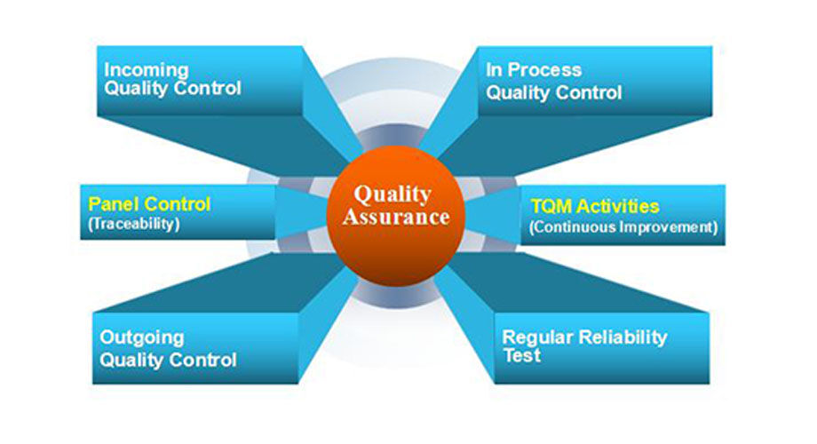
Quality Control
Customers Visit our factory

Exhibition Show
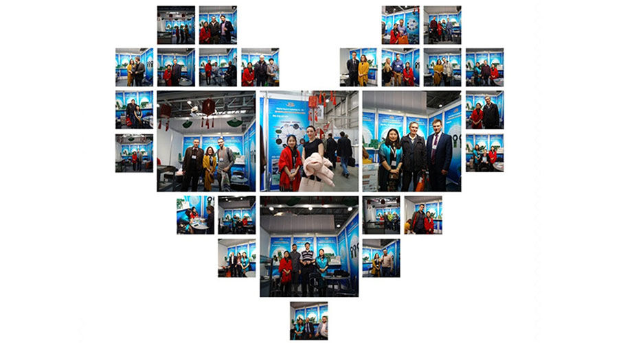
Munich Exhibition&Moscow
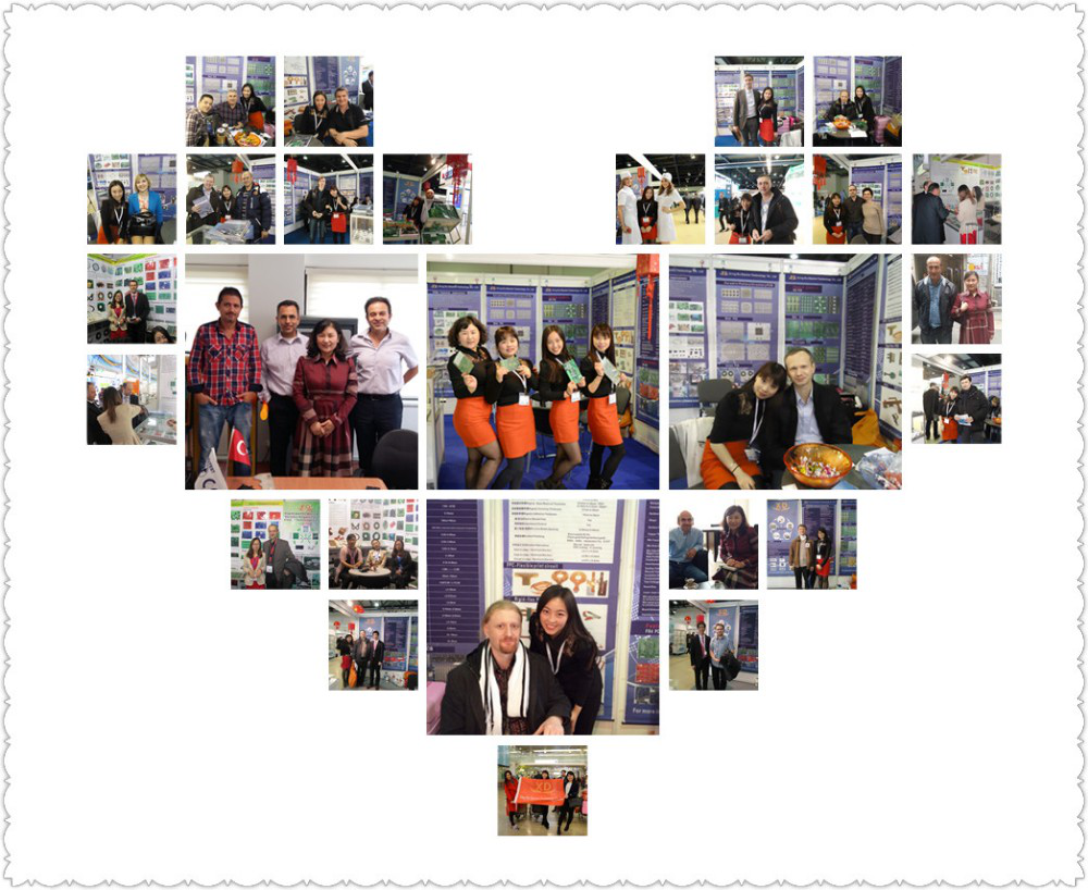
Russia Exhibition
Q1:Are you a factory or trade company?
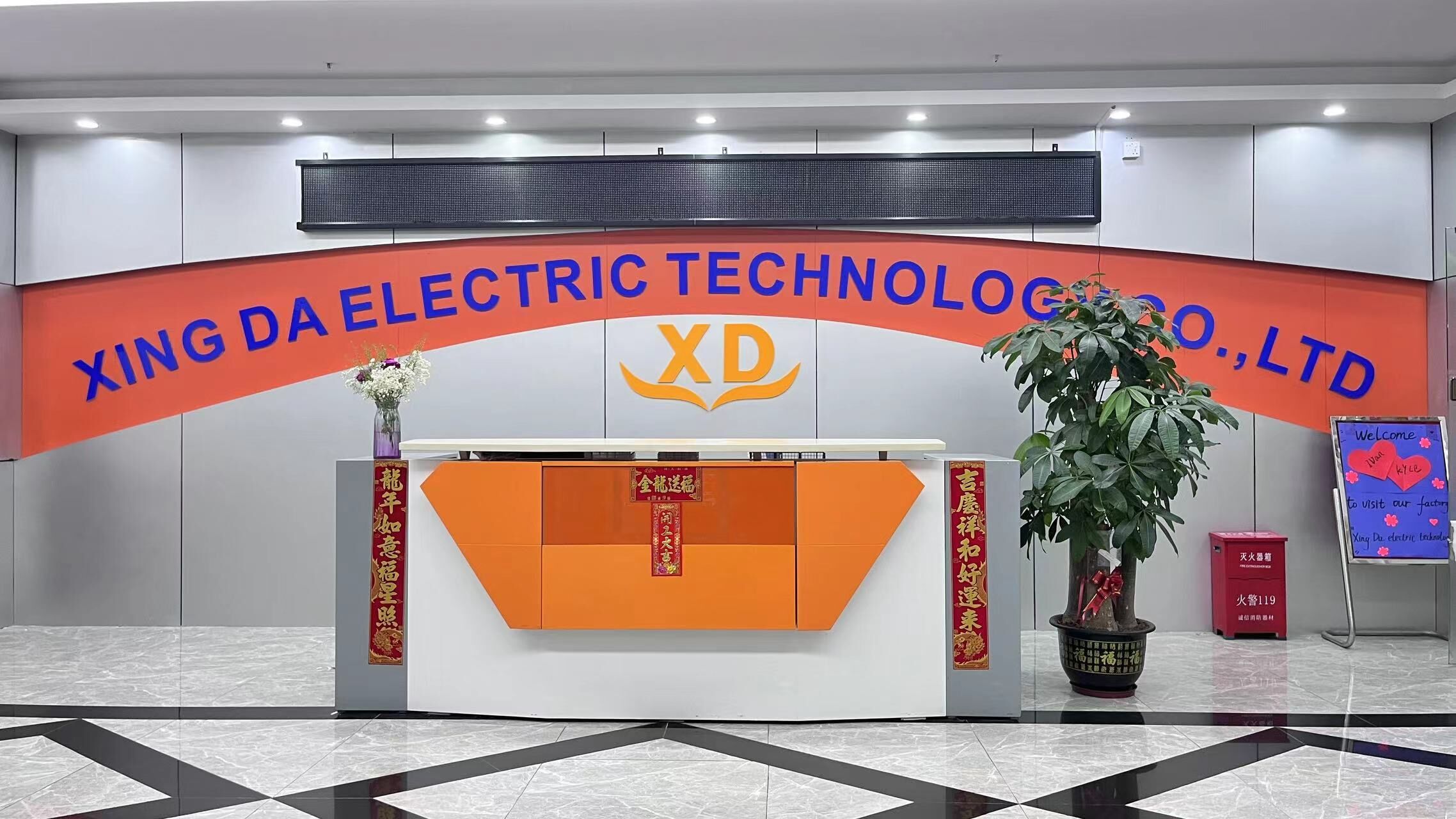
A: Xing Da Electronic Technology Co., ltd is leading OEM PCB&PCBA manufacturer in China with over 14 years rich experience. Our aim is “One-Stop service, smart manufacturing, make your production easier.”
Q2: What is needed for quotation?
A:1. PCB&FPC
We need ger ber files and specification for quotation
2. PCBA (= PCBA+ components + Assembly)
For PCBA, please send ger ber files, specification and Bom list for factory price.
Q3:Is my PCB or PCBA files safe if I send it to you for manufacturing?
A: We respect customer's design authority and will never manufacture PCB or PCBA for someone else without your permission. We never share customer documents with third parties.NDA is acceptable.
Q4:What payment do you accept ?
A: T/T,Western Union,Paypal, L/C,Credit Card, Cheque,Others
Q5: What's your shipping method?
A: 1. We have our own forwarders to ship goods with competitive price by DHL, UPS, FEDEX, TNT,EMS etc. We can also arrange shipments via sea or air depending on your specific requirements."
2. If you have your own forwarder, we can cooperate with them.
Q6: How about the MOQ?
A: There is no MOQ. We can produce prototypes, small orders, or large volumes.
Industrial HMI device PCBA OEM electronic printed circuit board pcb assembly pcb board customized pcba
Xing Da Electric Technology Co.,Ltd can provide one-stop service:
1. PCB layout
2. PCB manufacturing(1-38layers)
3. All electronic components purchasing
4. PCB assembling
5. PCBA function testing
6. Make mold of housing
7. Make housing and housing assembly.
PCB Product Capacity
| Item | Specification |
| Material | FR-4,FR1, CEM-1, CEM-3,Aluminum, Ceramic, Metal-backed Laminate, etc.Also make Crockery, Taconic, Rogers PCBs etc. |
| Remarks | High Tg CCL is Available(Tg>=180℃) |
| Finish Board Thickness | 0.2 mm-6.00mm(8mil-126mil) |
| Surface Finish | Gold finger(>=0.13um), Immersion Gold(0.025-0075um), Plating Gold(0.025-3.0um), HASL(5-20um), OSP(0.2-0.5um) |
| Shape | Routing、Punch、V-cut、Chamfer |
| Surface Treatment | Solder Mask(black, green, white, red, blue, thickness>=12um, Block, BGA) |
| Silkscreen(black, yellow, white) | |
| Peel able-mask(red, blue, thickness>=300um) | |
| Minimum Core | 0.075mm(3mil) |
| Copper Thickness | 1/2 oz min; 12oz max |
| Min Trace Width & Line Spacing | 0.075mm/0.0.075mm(3mil/3mil) |
| Min Hole Diameter for CNC Drilling | 0.1mm(4mil) |
| Min Hole Diameter for Punching | 0.6mm(35mil) |
| Biggest panel size | 610mm * 508mm |
| Hole Position | +/-0.075mm(3mil) CNC Drilling |
| Conductor Width(W) | +/-0.05mm(2mil) or +/-20% of original |
| Hole Diameter(H) | PTHL:+/-0.075mm(3mil) |
| Non PTHL:+/-0.05mm(2mil) | |
| Outline Tolerance | +/-0.1mm(5mil) CNC Routing |
| Warp & Twist | 0.70% |
| Insulation Resistance | 10Kohm-20Mohm |
| Conductivity | <50ohm |
| Test Voltage | 10-300V |
| Panel Size | 110 x 100mm(min) |
| 660 x 600mm(max) | |
| Layer-layer misregistration | 4 layers:0.15mm(6mil)max |
| 6 layers:0.25mm(10mil)max | |
| Min spacing between hole edge to circuitry pattern of an inner layer | 0.25mm(10mil) |
| Min spacing between board outline to circuitry pattern of an inner layer | 0.25mm(10mil) |
| Board thickness tolerance | 4 layers:+/-0.13mm(5mil) |
Flexible PCB Capacity
| FPC Tech Specification | |
| Items | Capabilities |
| Layers | FPC:1 to 6 Layers, Rigid Flex: 2 to 10 Layers |
| Regular Base Materials | Kapton,Polyimide(PI), Polyester(PET) |
| Base Copper Thickness | 1/3 oz to 8oz |
| Regular Base Material Thickness | 12.5um to 50um(FPC) |
| 0.1mm to 3.2mm(Rigid) | |
| Regular Coverlay Thickness | 27um to 50um |
| Regular Adhesive Thickness | 12um to 25um |
| Blind or Buried Vias | Yes |
| Impedance Control | Yes |
| Min.Line Width/Spacing | 0.04mm/0.04mm |
| Surface Finishing | Electroplate Ni/Au(Flash gold/Soft gold/Hard gold), ENIG, HASL, Immersion Tin,OSP |
| Outline Fabrication | Die cut, laser cut, CNC routing, V-scoring |
| Hole to edge(Hard tool/Die Cut) | ±0.1/±0.2mm |
| Edge to edge(Hard tool/Die Cut) | ±0.05/±0.2mm |
| Circuit to edge(Hard tool/Die Cut) | ±0.07/±0.2mm |
PCB Assembly(SMT) Product Capacity
| SMT Capacity | |
| SMT Item | Capacity |
| PCB Max. size | 510mm*1200mm(SMT) |
| Chip component | 01005,0201, 0402, 0603, 0805, 1206 package |
| Min.pin space of IC | 0.1mm |
| Min. space of BGA | 0.1mm |
| Max.precision of IC assembly | ±0.01mm |
| Assembly capacity | ≥8 million pionts/day |
| DIP capacity | 6 DIP production lines |
| Assembly testing | Bridge test,AOI test, X-Ray test, ICT(In Circuit Test) |
| FCT(Functional Circuit Test) | Current test, voltage test, high temperature and low temperature test,Drop Impact Test,aging test,water proof test,leakage-proof test and etc.Different test can be done according to your requirement. |
Quality Control
Customers Visit our factory
Exhibition Show
Munich Exhibition&Moscow
Russia Exhibition
Q1:Are you a factory or trade company?
A: Xing Da Electronic Technology Co., ltd is leading OEM PCB&PCBA manufacturer in China with over 14 years rich experience. Our aim is “One-Stop service, smart manufacturing, make your production easier.”
Q2: What is needed for quotation?
A:1. PCB&FPC
We need ger ber files and specification for quotation
2. PCBA (= PCBA+ components + Assembly)
For PCBA, please send ger ber files, specification and Bom list for factory price.
Q3:Is my PCB or PCBA files safe if I send it to you for manufacturing?
A: We respect customer's design authority and will never manufacture PCB or PCBA for someone else without your permission. We never share customer documents with third parties.NDA is acceptable.
Q4:What payment do you accept ?
A: T/T,Western Union,Paypal, L/C,Credit Card, Cheque,Others
Q5: What's your shipping method?
A: 1. We have our own forwarders to ship goods with competitive price by DHL, UPS, FEDEX, TNT,EMS etc. We can also arrange shipments via sea or air depending on your specific requirements."
2. If you have your own forwarder, we can cooperate with them.
Q6: How about the MOQ?
A: There is no MOQ. We can produce prototypes, small orders, or large volumes.
 ,Manufacturer ,Other